
Place of Origin:
Wuhan China
Brand Name:
Springtek
Certification:
ISO9001 RoHS FCC CE
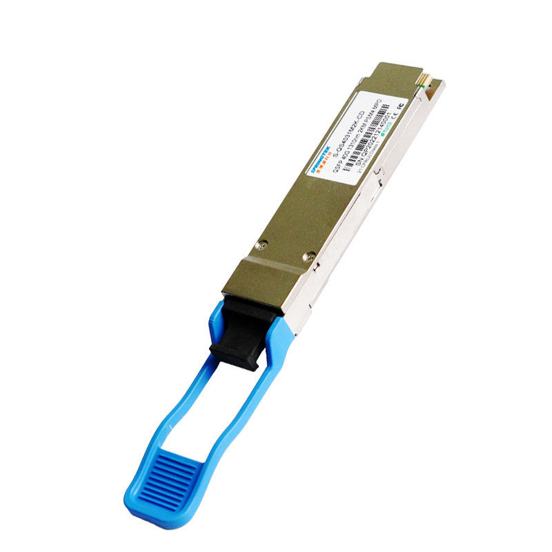
Model Number:
S-QS4031M2K-CD
40G QSFP+ IR4 1310nm 2km PSM MPO Compatible single-mode 40G Ethernet/ Infiniband QDR, DDR and SDR/Data Center
Ordering information
| Part Number | Product Description |
| S-QS4031M2K-CD | QSFP+, 40Gbps,PSM4,1310nm, SM, MPO, 2km, 0ºC ~ +70ºC, With DDM |
Description
Springtek QSFP+ 40G-PSM4 transceiver is designed to meet the requirements of 40G ethernet links over SMF up to 2km. It is compliant with QSFP+ MSA, IEEE 802.3ba. It is cost-effective, low power consumption with a single 3.3V power supply. It is fabricated with all-metal and compact size housing for superior EMI performance.
Features
Up to 11.2 Gbps data rate per channel
MPO optical connector (IEC61754-7-1)
Low power consumption 3.5W (max.)
Transmission length up to 2km
Transmitter with 4 channel 1310nm DFB laser
Receiver with 4 channel PIN photo detector
Operating case temperature:0 to 70 °C
RoHS compliant (lead free)
Applications
Switch Router and HBA’s
40G Ethernet
Infiniband QDR, DDR and SDR
High-performance Backplane
Absolute Maximum Ratings
| Parameter | Symbol | Min | Typ | Max | Unit |
| Power Supply Voltage | Vcc | 0 | 3.8 | V | |
| Storage Temperature Range | Ts | -40 | 85 | °C | |
| Relative Humidity - Storage | RHS | 0 | 95 | % | |
| Relative Humidity - Operating | RHO | 0 | 85 | % |
Recommended Operating Conditions
|
Electrical Characteristics
|
|||||||||||||||||||||||||||||||||||||||||||||||||||||||||||||||||||||||||||||||||||||||||||||||||||||||||||||||||||||||||||
Optical Characteristics
| Parameter | Symbol | Min | Typ | Max | Unit | Notes | |
| Transmitter Characteristics | |||||||
| Laser Type | DFB | ||||||
| Data Rate per lane | - | - | 10.3125 | - | Gb/s | ||
| Lane Center Wavelengths | λ0 | 1260 | 1360 | nm | |||
| Side-mode suppression ratio | SMSR | 30 | - | - | dB | ||
| Total average Launch Power | PT | - | - | 5 | dBm | ||
| Average Launch Power, each lane | POUT | -8.2 | - | 0.5 | dBm | ||
| Optical Modulation Amplitude, each lane | OMA | -5.2 | - | 2.0 | dBm | ||
| Difference in launch power between any two lanes (OMA) | - | - | 5 | dB | |||
| Launch Power in OMA minus TDP, each lane | -4.8 | - | - | dBm | |||
| Extinction Ratio | ER | 3.5 | - | - | dB | ||
| Transmitter dispersion penalty | TDP | - | - | 2.6 | dB | ||
| Average Launch Power of OFF transmitter, each lane | POFF | - | - | -30 | dBm | ||
| Relative Intensity Noise | RIN | - | - | -128 | dB/Hz | ||
| Optical return loss tolerance | - | - | 12 | dB | |||
| Transmitter eye mask definition | Compliant to IEEE802.3ba | ||||||
| Receiver Characteristics | |||||||
| Receiver Type | PIN | ||||||
| Lane Center Wavelengths | λ | 1260 | 1360 | nm | |||
| Average receive power, each lane | PIN1 | -12.6 | - | 2.3 | dBm | ||
| Damage Threshold | DT | 3 | - | - | dBm | ||
| Receiver Sensitivity (OMA), each lane (max) | Sen1 | - | - | -12.6 | dBm | 1 | |
| LOS Assert | LOSA | -30 | - | - | dBm | ||
| LOS De-Assert | LOSD | - | - | -15 | dBm | ||
| LOS Hysteresis | LOSH | 0.5 | - | 6 | dB | ||
| Notes | |||||||
| 1. BER=1E-12, measured with PRBS31@10.3125Gbps | |||||||
General Specifications
| Pin | Symbol | Name/Description | Notes |
| 1 | GND | Ground | |
| 2 | Tx2n | Transmitter Inverted Data Input | |
| 3 | Tx2p | Transmitter Non-Inverted Data Input | |
| 4 | GND | Ground | |
| 5 | Tx4n | Transmitter Inverted Data Input | |
| 6 | Tx4p | Transmitter Non -Inverted Data Input | |
| 7 | GND | Ground | |
| 8 | ModselL | Module Select | |
| 9 | RetsetL | Module Reset | |
| 10 | VCC Rx | +3.3V Power Supply Receiver | |
| 11 | SCL | 2-wire serial interface clock | |
| 12 | SDA | 2-wire serial interface data | |
| 13 | GND | Ground | |
| 14 | Rx3p | Receiver Non-Inverted Data Output | |
| 15 | Rx3n | Receiver Inverted Data Output | |
| 16 | GND | Ground | |
| 17 | Rx1p | Receiver Non-Inverted Data Output | |
| 18 | Rx1n | Receiver Inverted Data Output | |
| 19 | GND | Ground | |
| 20 | GND | Ground | |
| 21 | Rx2n | Receiver Inverted Data Output | |
| 22 | Rx2p | Receiver Non-Inverted Data Output | |
| 23 | GND | Ground | |
| 24 | Rx4n | Receiver Inverted Data Output | |
| 25 | Rx4p | Receiver Non-Inverted Data Output | |
| 26 | GND | Ground | |
| 27 | ModPrsL | Module Present | |
| 28 | IntL | Interrupt | |
| 29 | VCC Tx | +3.3V Power Supply transmitter | |
| 30 | VCC1 | +3.3V Power Supply | |
| 31 | LPMode | Low Power Mode | |
| 32 | GND | Ground | |
| 33 | Tx3p | Transmitter Non-Inverted Data Input | |
| 34 | Tx3n | Transmitter Inverted Data Input | |
| 35 | GND | Ground | |
| 36 | Tx1p | Transmitter Non-Inverted Data Input | |
| 37 | Tx1n | Transmitter Inverted Data Input | |
| 38 | GND | Ground |
Send your inquiry directly to us