
Place of Origin:
Wuhan China
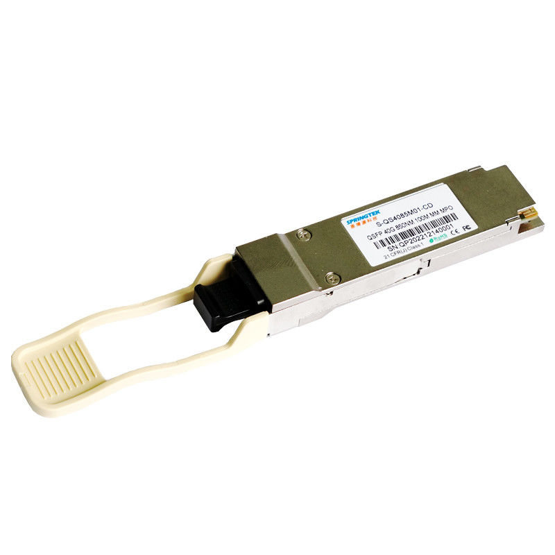
Brand Name:
Springtek
Certification:
ISO9001 RoHS FCC CE
Model Number:
S-QS4085M01-CD
40G MM Compatible Arista QSFP+ 850nm 100M MPO Optical Transceiver Module
Ordering information
| Part Number | Product Description |
| S-QS4085M01-CD | QSFP+, 40Gbps, 850nm, MM, MPO,100m, 0ºC~+70ºC, With DDM |
Description
Springtek 40G SR4 QSFP+ transceiver is designed to meet the requirements of 40G ethernet including breaking out to 10G SR links over OM3 MMF up to 100m. It is compliant with QSFP+ MSA, IEEE 802.3ba. It is cost-effective, low power consumption with a single 3.3V power supply. It is fabricated with all-metal and compact size housing for superior EMI performance.
Features
Single +3.3V power supply
Operating Temperature:0 to +70°C
RoHS compliant (lead free)
Applications
40G-IB-QDR /20G-IB-DDR / 10G-IB-SDR InfniBand
Breakout to 4 x 10GBASE-SR
Absolute Maximum Ratings
| Parameter | Symbol | Min | Typ | Max | Unit |
| Power Supply Voltage | Vcc | -0.5 | 4 | V | |
| Storage Temperature Range | Ts | -40 | 85 | °C | |
| Relative Humidity - Storage | RHS | 0 | 95 | % | |
| Relative Humidity - Operating | RHO | 0 | 85 | % |
Recommended Operating Conditions
| Parameter | Symbol | Min | Typ | Max | Unit |
| Case Operating Temperature Range | Tc | 0 | - | 70 | °C |
| Power Supply Voltage | Vcc | 3.14 | 3.3 | 3.46 | V |
| Total Power Consumption | P | - | - | 1.5 | W |
| Data Rate | BR | - | 10.3125 | - | Gbps |
Electrical Characteristics
| Parameter | Symbol | Min | Typ | Max | Unit | Note | ||
| Differential Input Voltage Swing | VIN | 180 | - | 1200 | mV | |||
| Tx Differential Input Impendence | ZIN | - | 100 | - | Ω | |||
| Differential input return loss | Per IEEE P802.3ba 86A.4.1.1 | dB | 10MHz to 11.1GHz | |||||
| Differential to common-mode input return loss | 10 | - | - | dB | 10MHz to 11.1GHz | |||
| J2 Jitter Tolerance | J2T | 0.17 | - | - | UI | Per IEEE P802.3ba 86A.4.1 | ||
| J9 Jitter Tolerance | J9T | 0.29 | - | - | UI | |||
| Receiver Electrical Characteristics | ||||||||
| Parameter | Symbol | Min | Typ | Max | Unit | |||
| Differential output Voltage Swing | VOUT | 300 | - | 900 | mV | |||
| Rx Differential Output Impendence | ZOUT | - | 100 | - | Ω | |||
| Differential output return loss | Per IEEE P802.3ba 86A.4.2.1 | dB | 10MHz to 11.1GHz | |||||
| Common mode output return loss | Per IEEE P802.3ba 86A.4.2.2 | dB | 10MHz to 11.1GHz | |||||
| Output transition time,20% to 80% | 28 | - | - | ps | Per IEEE P802.3ba 86A.4.2 | |||
| J2 Jitter output | J2O | - | - | 0.42 | UI | |||
| J9 Jitter output | J9O | - | - | 0.65 | UI | |||
Optical Characteristics
| Parameter | Symbol | Min | Typ | Max | Unit | Notes |
| Transmitter Characteristics | ||||||
| Laser Type | VCSEL | |||||
| Center Wavelength | λ | 840 | 850 | 860 | nm | |
| RMS Spectral Width | ∆λ | - | - | 0.4 | nm | |
| Average Launch Power, each lane | POUT | -7.6 | - | 2.4 | dBm | |
|
Difference in launch power between any two lanes(OMA) |
DPx | - | - | 4 | dB | |
| Peak power, each lane | PPx | - | - | 4 | dBm | |
| Extinction Ratio | ER | 3 | - | - | dB | |
| Transmitter dispersion penalty | TDP | -- | -- | 3.5 | dB | |
| Average Launch Power of OFF transmitter, each lane | POFF | - | - | -30 | dBm | |
| Optical return loss tolerance | ORL | - | - | 12 | dB | |
|
Transmitter eye mask definition{X1,X2,X3,Y1,Y2,Y3} |
{0.23,0.34,0.43,0.27,0.35,0.4} | |||||
| Receiver Characteristics | ||||||
| Receiver Type per lane | PIN | |||||
| Receiver Wavelength | λ | 840 | 850 | 860 | nm | |
| Average power at receive input, each lane | PXPx | - 9.5 | - | 2.4 | dBm | |
| Stressed Receiver Sensitivity in OMA | SRS | - | - | -5.4 | dBm | 1 |
| LOS Assert | LOSA | -30 | - | - | dBm | |
| LOS De-Assert | LOSD | - | - | -12 | dBm | |
| LOS Hysteresis | LOSH | 0.5 | dB | |||
| Receiver Reflectance | Rfl | -12 | dB | |||
| Notes | ||||||
| 1.Measured with a PRBS 231 -1 test pattern, @10.3125Gb/s, BER<1E-12. | ||||||
Send your inquiry directly to us