
Place of Origin:
Wuhan China
Brand Name:
Springtek
Certification:
ISO9001 RoHS FCC CE
Model Number:
S-QP1AL4L40-CD-OTU4
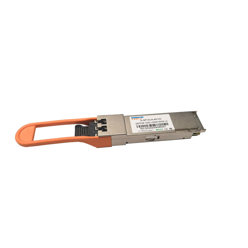
QSFP28 ER4 OTU4 Cisco Compatible 100Gbps 1294 -1310nm 40Km Optical Transceiver Module
Ordering information
| Part Number | Product Description |
|
S-QP1AL4L40-CD-OTU4 |
QSFP28, 103.1~111.8Gb/s ,1294-1310nm, LC,40km, OTU4, 0ºC~+70ºC, With DDM |
Description
Springtek 100G QSFP28 ER4 OTU4 optical Transceiver integrates receiver and transmitter path on one module. In the transmit side, four lanes of serial data streams are recovered, retimed, and passed to four laser drivers. The laser drivers control 4WDM EML with center wavelength of 1295.56 nm, 1300.05nm, 1304.58nm and 1309.14 nm. The optical signals are multiplexed to a single –mode fiber through an industry standard LC connector. In the receive side, the four lanes of optical data streams are optically de-multiplexed by the integrated optical de-multiplexer. Each data stream is recovered by a APD and trans-impedance amplifier, retimed. This module features a hot-pluggable electrical interface, low power consumption and 2-wire serial interface.
Springtek product is designed with form factor, optical/electrical connection and digital diagnostic interface according to the QSFP28 Multi-Source Agreement (MSA) and compliant to IEEE 802.3ba.
Features
Applications
Absolute Maximum Ratings
| Parameter | Symbol | Min | Typ | Max | Unit | Notes |
| Power Supply Voltage | Vcc | -0.5 | 3.6 | V | ||
| Storage Temperature Range | Ts | -40 | 85 | °C | ||
| Relative Humidity - Storage | RHS | 5 | 95 | % | ||
| Data Input Voltage – Differential | lVDIP-VDINl | - | - | 1.0 | V | |
| Control Input Voltage | VI | -0.3 | - | Vcc+0.5 | V | |
| Control Output Current | IO | -20 | - | 20 | mA |
Recommended Operating Conditions
| Parameter | Symbol | Min | Typ | Max | Unit | Notes |
| Case Operating Temperature Range | Tc | 0 | - | 70 | °C | |
| Power Supply Voltage | Vcc | 3.14 | 3.3 | 3.47 | V | |
| Total Power Consumption | PD | - | - | 4.5 | W | |
| Instantaneous peak current at hot plug | ICC_IP | - | - | 1800 | mA | |
| Sustained peak current at hot plug | ICC_SP | - | - | 1485 | mA | |
| Maximum Power Dissipation,Low Power Mode | PDLP | - | - | 1.5 | W | |
| Aggregate Bit Rate | ABR | - | 103.125 | 111.8 | Gb/s | |
| Data Rate per Lane | DRL | - | 25.78125 | - | Gb/s | |
| Control Input Voltage High | VIH | VCC*0.7 | - | VCC+0.3 | V | |
| Control Input Voltage Low | VIL | -0.3 | - | VCC+0.3 | V | |
| Two Wire Serial Interface Clock Rate | - | - | - | 400 | kHz | |
| Power Supply Noise Tolerance | - | - | - | 66 | mVpp | 10 Hz -10 MHz |
| Rx Differential Data Output Load | - | - | 100 | - | ohms | |
| Operating Distance | - | 2 | - | 40 | km | With FEC |
Electrical Specifications
| Transmitter (Module Input) | ||||||
| Parameter | Symbol | Min | Typ | Max | Unit | Notes |
| Differential Data Input Amplitude | VIN,P-P | 95 | - | 900 | mVpp | |
| Differential Termination Mismatch | - | - | 10 | % | ||
| LPMode, Reset and ModSelL | VIL | -0.3 | - | 0.8 | V | |
| VIH | 2 | - | VCC+0.3 | V | ||
| Receiver (Module Output) | ||||||
| Differential Data Output Amplitude | VOUT,P-P | 250 | - | 900 | mVpp | |
| Differential Termination Mismatch | - | - | % | |||
| Output Rise/Fall Time, 20%~80% | TR | 9.5 | - | 10 | ps | |
| ModPrsL and IntL | VOL | 0 | - | 0.4 | V | IOL=4mA |
| VOH | VCC-0.5 | - |
VCC+0.3
|
V | IOL=4mA | |
ptical Characteristics
| Transmitter Characteristics | ||||||
| Parameter | Symbol | Min | Typ | Max | Unit | Notes |
| Lane center wavelengths(range) | λ | 1294.53 | 1295.56 | 1296.59 | nm | |
| 1299.02 | 1300.05 | 1301.09 | ||||
| 1303.54 | 1304.58 | 1305.63 | ||||
| 1308.09 | 1309.14 | 1310.19 | ||||
| Side Mode Suppression Ratio | SMSR | 30 | - | - | dB | |
| Total Average Optical Launch Power, 100GE | POUT | - | - | 12.5 | dBm | |
| Average Launch Power, each lane, 100GE | POUTL | -2.5 | - | 6.5 | dBm | |
| Total Average Optical Launch Power, OTU4 | - | - | 11.1 | dBm | ||
| Average Optical Launch Power per Lane, OTU4 | POUTL | 0.6 | - | 5.1 | dBm | |
| Average Launch Power of OFF transmitter, each lane | POUT_OFF | - | - | -30 | dBm | |
| Extinction Ratio | ER | 7 | - | - | dB | |
| Optical Modulation Amplitude (OMA) per Lane, 100GE | OMA | 0.5 | - | 6.5 | dBm | |
| Launch Power in OMA minus TDP per Lane, 100GE | OMA-TDP | -0.5 | - | - | dBm | |
| Difference in launch power between any two lanes (Average and OMA) | DT_OMA | - | - | 4 | dB | |
| Transmitter and Dispersion Penalty, 100GE | TDP | - | - | 3 | dB | |
| Optical Path Penalty, OTU4 | OPP | - | - | 1.5 | dB | |
| Optical Return Loss Tolerance | ORLT | 20 | - | - | dB | |
| Optical Eye Mask, 100GE | Compliant with IEEE 802.3ba-2010 | 1 | ||||
| Optical Eye Mask, OTU4 | Compliant with ITU-T G.695 | 2 | ||||
| Transmitter Reflectance | TR | - | - | -26 | dB | |
| Receiver Characteristics | ||||||
| Parameter | Symbol | Min | Typ | Max | Unit | Notes |
| Lane center wavelengths(range) | λ | 1294.53 | 1295.56 | 1296.59 | nm | |
| 1299.02 | 1300.05 | 1301.09 | ||||
| 1303.54 | 1304.58 | 1305.63 | ||||
| 1308.09 | 1309.14 | 1310.19 | ||||
| Receiver Sensitivity (OMA), each lane, 100GE | - | - | - | -18.5 | dBm | 3 |
| Receiver Sensitivity (Average Power) per Lane, OTU4 | - | - | - | -18.99 | dBm | 4 |
| Stressed receiver sensitivity (OMA), per Lane, 100GE | - | - | - | -16 | dBm | |
| Stressed Eye J2 Jitter | - | - | 0.33 | - | UI | |
| Stressed Eye J4 Jitter | - | 0.48 | - | UI | ||
| Vertical Eye Closure Penalty | - | - | 2.5 | - | dB | |
| SRS eye mask definition { X1, X2, X3,Y1, Y2, Y3} | {0.39, 0.5, 0.5, 0.39, 0.39, 0.4} | |||||
| Damage threshold, each lane | Pin, damage | -2.5 | - | - | dBm | |
| Average Receive Power per Lane | - | -20.5 | - | -3.5 | dBm | |
|
Receive Power in OMA per Lane, Overload |
OMA | - | - | -3.5 | dBm | |
| Receiver Reflectance | TR | - | - | -26 | dB | |
|
Notes 1. Measured with a PRBS 231-1 test pattern @25.78 Gb/s. 2. Measured with a PRBS 231-1 test pattern @27.95 Gb/s 3. Measured with a PRBS231-1 test pattern @25.78Gbps, BER≦5E-5 4. Measured with a PRBS231-1 test pattern @27.95Gbps, BER≦1.8E-4. |
||||||
Send your inquiry directly to us