
Place of Origin:
Wuhan China
Brand Name:
Springtek
Certification:
ISO9001 RoHS FCC CE
Model Number:
S-QS40C4L20-CD
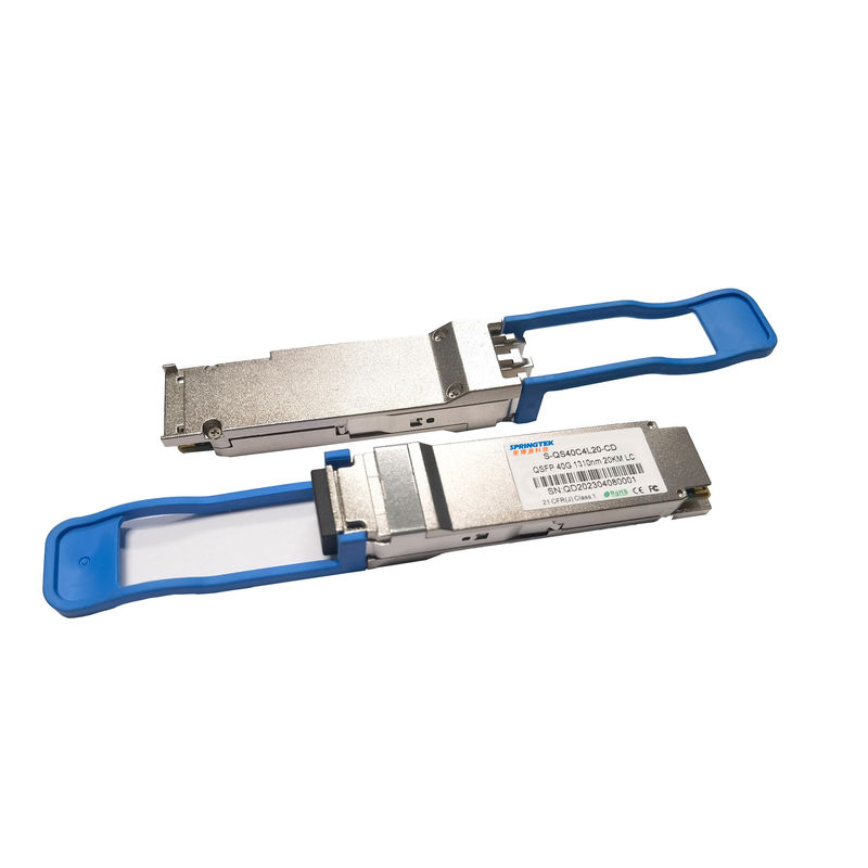
Compatible Cisco 40Gbps QSFP+ 1310nm 20KM LC Optical Transceiver Module
Ordering information
| Part Number | Product Description |
| S-QS40C4L20-CD | QSFP+, 40Gbps,1310nm, SM,LC,20km, 0ºC ~ +70ºC, With DDM |
Description
Springtek 40G-LR4 QSFP+ transceiver is designed to meet the requirements of 40G ethernet links over SMF up to 20km. It is compliant with QSFP+ MSA, IEEE 802.3ba 40GBase-LR4. It is cost-effective, low power consumption with a single 3.3V power supply. It is fabricated with all-metal and compact size housing for superior EMI performance.
Features
Supports bit rate up to 10.3125Gb/s per lane
Duplex LC interface
Uncooled 4x10Gbps CWDM transmitter, PIN array detector
Low power consumption <3.5W
Maximum link length of 20km on Single Mode Fiber (SMF)
All-metal housing for superior EMI performance
IIC management interface
Single +3.3V power supply
Operating case temperature:0 to 70 °C
RoHS compliant (lead free)
Applications
High speed accesss
Absolute Maximum Ratings
| Parameter | Symbol | Min | Typ | Max | Unit |
| Power Supply Voltage | Vcc | -0.5 | 4 | V | |
| Storage Temperature Range | Ts | -40 | 85 | °C | |
| Relative Humidity - Storage | RHS | 0 | 95 | % | |
| Relative Humidity - Operating | RHO | 0 | 85 | % |
Recommended Operating Conditions
| Parameter | Symbol | Min | Typ | Max | Unit |
| Case Operating Temperature Range | Tc | 0 | - | 70 | °C |
| Power Supply Voltage | Vcc | 3.14 | 3.3 | 3.47 | V |
| Total Power Consumption | P | - | - | 3.5 | W |
| Data Rate per Lane | BR | - | 10.3125 | - | Gbps |
Electrical Characteristics
| Transmitter Electrical Characteristics | ||||||
| Parameter | Symbol | Min | Typ | Max | Unit | Note |
| Differential Input Voltage Swing | VIN | 180 | - | 1200 | mV | |
| Tx Differential Input Impendence | ZIN | - | 100 | - | Ω | |
| Differential input return loss | Per IEEE P802.3ba 86A.4.1.1 | dB | 10MHz to 11.1GHz | |||
| Differential to common-mode input return loss | 10 | - | - | dB | 10MHz to 11.1GHz | |
| J2 Jitter Tolerance | J2T | 0.17 | - | - | UI | Per IEEE P802.3ba 86A.4.1 |
| J9 Jitter Tolerance | J9T | 0.29 | - | - | UI | |
| Receiver Electrical Characteristics | ||||||
| Parameter | Symbol | Min | Typ | Max | Unit | |
| Differential output Voltage Swing | VOUT | 300 | - | 1200 | mV | |
| Rx Differential Output Impendence | ZOUT | - | 100 | - | Ω | |
| Differential output return loss | Per IEEE P802.3ba 86A.4.2.1 | dB | 10MHz to 11.1GHz | |||
| Common mode output return loss | Per IEEE P802.3ba 86A.4.2.2 | dB | 10MHz to 11.1GHz | |||
| Output transition time,20% to 80% | 28 | - | - | ps | Per IEEE P802.3ba 86A.4.2 | |
| J2 Jitter output | J2O | - | - | 0.42 | UI | |
| J9 Jitter output | J9O | - | - | 0.65 | UI | |
Optical Characteristics
| Parameter | Symbol | Min | Typ | Max | Unit | Notes | |
| Transmitter Characteristics | |||||||
| Laser Type | CWDM DFB | ||||||
| Data Rate per lane | - | - | 10.3125 | - | Gb/s | ||
|
Lane Center Wavelengths
|
λ0 | 1264.5 | 1277.5 | nm | |||
| λ1 | 1284.5 | 1297.5 | |||||
| λ2 | 1304.5 | 1317.5 | |||||
| λ3 | 1324.5 | 1337.5 | |||||
| Side-mode suppression ratio | SMSR | 30 | - | - | dB | ||
| Total average Launch Power | PT | - | - | 8.3 | dBm | ||
| Average Launch Power, each lane | POUT | -4.5 | - | 2.3 | dBm | ||
| Optical Modulation Amplitude, each lane | OMA | -4 | - | 3.5 | dBm | ||
| Difference in launch power between any two lanes (OMA) | - | - | 6.5 | dB | |||
| Launch Power in OMA minus TDP, each lane | -4.8 | - | - | dBm | |||
| Extinction Ratio | ER | 3.5 | - | - | dB | ||
| Transmitter dispersion penalty | TDP | - | - | 2.6 | dB | ||
| Average Launch Power of OFF transmitter, each lane | POFF | - | - | -30 | dBm | ||
| Relative Intensity Noise | RIN | - | - | -128 | dB/Hz | ||
| Optical return loss tolerance | - | - | 20 | dB | |||
| Transmitter Reflectance | - | - | -12 | dB | |||
| Transmitter eye mask definition | Compliant to IEEE802.3ba | ||||||
| Receiver Characteristics | |||||||
| Receiver Type | PIN | ||||||
| Data Rate per lane | - | 10.3125 | - | Gb/s | |||
| Lane Center Wavelengths | λ0 | 1264.5 | 1277.5 | nm | |||
| λ1 | 1284.5 | 1297.5 | |||||
| λ2 | 1304.5 | 1317.5 | |||||
| λ3 | 1324.5 | 1337.5 | |||||
| Average receive power, each lane | PIN1 | -13.7 | - | 2.3 | dBm | ||
| Damage Threshold | DT | 3.3 | - | - | dBm | ||
| Receiver Power (OMA), each lane (max) | - | - | 3.5 | dBm | |||
| Difference in receive power between any two lanes(OMA)(max) | - | - | 7.5 | dB | |||
| Receiver Sensitivity (OMA), each lane (max) | Sen1 | - | - | -11.5 | dBm | 1 | |
| Stressed Receiver Sensitivity (OMA), each lane (max) | Sen1 | - | - | -9.6 | dBm | ||
| Receiver 3dB electrical upper cutoff frequency, each lane | - | - | 12.3 | GHz | |||
| Receiver Reflectance | RFL | - | - | -26 | dB | ||
| LOS Assert | LOSA | -30 | - | - | dBm | ||
| LOS De-Assert | LOSD | - | - | -15 | dBm | ||
| LOS Hysteresis | LOSH | 0.5 | 3 | 5 | dB | ||
| Notes | |||||||
| 1. BER=1E-12, measured with PRBS31@10.3125Gbps | |||||||
Send your inquiry directly to us