
Place of Origin:
Wuhan China
Brand Name:
Springtek
Certification:
ISO9001 RoHS FCC CE
Model Number:
S-QD4A85M01-CD-8
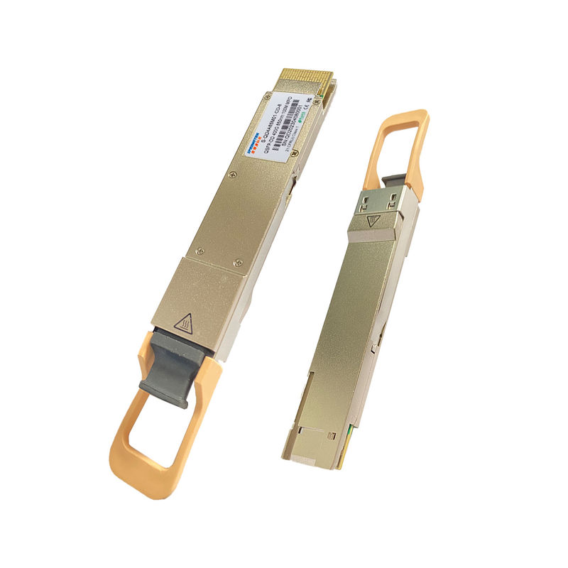
400GMPO/MTP 850nm Juniper Compatible QSFP-DD SR8 100M Optical Transceiver
QSFP-DD SR8 S-QD4A85M01-CD-8 230301.pdf
Ordering information
| Part Number | Product Description |
| S-QD4A85M01-CD-8 | QSFP-DD 400G 850nm SR8 100M MPO, 0ºC~+70ºC, With DDM |
Description
Springtek 400Gb/s QSFP-DD SR8 optical module. It provides increased port density and total system cost savings. The QSFP-DD full duplex optical module offers 8 independent transmit and receive channels, each capable of 53.125Gb/s operation for an aggregate data rate of 400Gb/s on 100 meters of OM3 multi-mode fiber.
An optical fiber cable with an MTP/MPO-16 connector can be plugged into the QSFP-DD SR8 module receptacle. Proper alignment is ensured by the guide pins inside the receptacle. The cable usually cannot be twisted for proper channel to channel alignment. Electrical connection is achieved through an QSFP-DD MSA-compliant edge type connector.
The central wavelengths of all the 8 parallel lanes are 850nm. It contains an optical MPO-16 connector for the optical interface and a 60-pin connector for the electrical interface. Host FEC is required to support up to 70m OM3 multi-mode fiber transmission.
S-QD4A85M01-CD-8 product is designed with form factor, optical/electrical connection and digital diagnostic interface according to the QSFP-DD Multi-Source Agreement (MSA) Type 2. It has been designed to meet the harshest external operating conditions including temperature, humidity and EMI interference.
Features
Applications
Absolute Maximum Ratings
It hasto be noted that the operation in excess of any individual absolute maximum ratings might cause permanent damage to this module.
| Parameter | Symbol | Min | Typ | Max | Unit |
| Power Supply Voltage | Vcc | -0.5 | 3.6 | V | |
| Storage Temperature Range | Ts | -40 | 85 | °C | |
| Operating Case Temperature | To | 0 | 70 | °C | |
| Relative Humidity (non-condensation) | RH | 0 | 85 | % |
Recommended Operating Conditions and Power Supply Requirements
| Parameter | Symbol | Min | Typical | Max | Units | Notes |
| Operating Case Temperature | TOP | 0 | 70 | degC | ||
| Power Supply Voltage | VCC | 3.135 | 3.3 | 3.465 | V | |
| Data Rate, each Lane | 26.5625 | GBd | PAM4 | |||
| Data Rate Accuracy | -100 | 100 | ppm | |||
| Pre-FEC Bit Error Ratio | 2.4x10⁻⁴ | |||||
| Post-FEC Bit Error Ratio | 1x10-12 | 1 | ||||
| Link Distance with OM3 | D | 0.5 | 100 | m | 2 |
Notes:
1. FEC provided by host system.
2. FEC required on host system to support maximum distance.
Electrical Characteristics
The following electrical characteristics are defined over the Recommended Operating Environment unless otherwise specified.
| Parameter | Test Point | Min | Typical | Max | Units | Notes |
| Power Consumption | 12 | W | ||||
| Supply Current | Icc | 3.63 | A | |||
| Transmitter (each Lane) | ||||||
| Signaling Rate, each Lane | TP1 | 26.5625 ± 100 ppm | GBd | |||
|
Differential pk-pk Input Voltage Tolerance Mismatch |
TP1a | 900 | mVpp | 1 | ||
| Differential Termination | TP1 | 10 | % | |||
| Differential Input Return Loss | TP1 |
IEEE 802.3-2015 Equation (83E-5) |
dB | |||
| Differential to Common Mode Input Return Loss |
TP1 | IEEE 802.3-2015 Equation (83E-6) |
dB | |||
| Transition Time, 20% to 80% | TP4 | 9.5 | ps | |||
|
Near-end Eye Symmetry Mask Width (ESMW) |
TP4 | 0.265 | UI | |||
| Near-end Eye Height, Differential | TP4 | 70 | mV | |||
|
Far-end Eye Symmetry Mask Width (ESMW) |
TP4 | 0.2 | UI | |||
| Far-end Eye Height, Differential | TP4 | 30 | mV | |||
| Far-end Pre-cursor ISI Ratio | TP4 | -4.5 | 2.5 | % | ||
| Common Mode Output Voltage (Vcm) | TP4 | -350 | 2850 | mV | 3 | |
Notes:
1. With the exception to IEEE 802.3bs 120E.3.1.2 that the pattern is PRBS31Q or scrambled idle.
2. Meets BER specified in IEEE 802.3bs 120E.1.1.
3. DC common mode voltage generated by the host. Specification includes effects of ground offset voltage.
Optical Characteristics
| Parameter | Symbol | Min | Typical | Max | Units | Notes |
| Transmitter | ||||||
| Center Wavelength | λC | 840 | 850 | 860 | nm | |
| Data Rate, each Lane | 26.5625 ± 100 ppm | GBd | ||||
| Modulation Format | PAM4 | |||||
| RMS Spectral Width | ∆λrms | 0.6 | nm | Modulated | ||
| Average Launch Power, each Lane | PAVG | -6.5 | 4 | dBm | 1 | |
|
Outer Optical Modulation Amplitude (OMAouter), each Lane |
POMA | -4.5 | 3 | dBm | 2 | |
|
Launch Power in OMAouter minus TDECQ, each Lane |
-5.9 | dB | ||||
|
Transmitter and Dispersion Eye Clouser for PAM4, each Lane |
TDECQ | 4.5 | dB | |||
| Extinction Ratio | ER | 3 | dB | |||
| Optical Return Loss Tolerance | TOL | 12 | dB | |||
|
Average Launch Power of OFF Transmitter, each Lane |
Poff | -30 | dBm | |||
| Encircled Flux |
≥ 86% at 19 μm ≤ 30% at 4.5 μm |
|||||
| Receiver | ||||||
| Center Wavelength | λC | 840 | 850 | 860 | nm | |
| Data Rate, each Lane | 26.5625 ± 100 ppm | GBd | ||||
| Modulation Format | PAM4 | |||||
| Damage Threshold, each Lane | THd | 5 | dBm | 3 | ||
| Average Receive Power, each Lane | -7.9 | 4 | dBm | 4 | ||
| Receive Power (OMAouter), each Lane | 3 | dBm | ||||
| Receiver Sensitivity | SEN | -6.5 | dBm | 5 | ||
| (OMAouter), each Lane | ||||||
| Stressed Receiver Sensitivity(OMAouter), each Lane | SRS | -3 | dBm | 6 | ||
| Receiver Reflectance | RR | -12 | dB | |||
| LOS Assert | LOSA | -30 | dBm | |||
| LOS De-assert | LOSD | -12 | dBm | |||
| LOS Hysteresis | LOSH | 0.5 | dB | |||
| Stressed Conditions for Stress Receiver Sensitivity (Note 7) | ||||||
| Stressed Eye Closure for PAM4 (SECQ), Lane under Test |
4 | dB | ||||
| OMAouter of each Aggressor Lane | 3 | dBm | ||||
Notes:
1. Average launch power, each lane (min) is informative and not the principal indicator of signal strength. A transmitter with launch power below this value cannot be compliant; however, a value above this does not ensure compliance.
2. Even if the TDECQ < 1 dB , the OMAouter (min) must exceed the minimum value specified here.
3. The receiver shall be able to tolerate, without damage, continuous exposure to an optical input signal having this average power level.
4. Average receive power, each lane (min) is informative and not the principal indicator of signal strength. A received power below this value cannot be compliant; however, a value above this does not ensure compliance.
5. Receiver Sensitivity OMAouter, each lane (max) is informative and is defined for a BER of 2.4x10⁻⁴.
6. Measured with conformance test signal at receiver input for the BER of 2.4x10⁻⁴.
7. These test conditions are for measuring stressed receiver sensitivity. They are not characteristics of the receiver.
Digital Diagnostic Functions
The following digital diagnostic characteristics are defined over the normal operating conditions unless otherwise specified.
| Parameter | Symbol | Min | Max | Units | Notes |
| Temperature monitor absolute error | DMI_Temp | -3 | 3 | degC | Over operating temperature range |
| Supply voltage monitor absolute error | DMI _VCC | -0.1 | 0.1 | V | Over full operating range |
|
Channel RX power monitor absolute error |
DMI_RX_Ch | -2 | 2 | dB | 1 |
| Channel Bias current monitor | DMI_Ibias_Ch | -10% | 10% | mA | |
|
Channel TX power monitor absolute error |
DMI_TX_Ch | -2 | 2 | dB | 1 |
Notes:
1. Due to measurement accuracy of different fibers, there could be an additional +/-1 dB fluctuation, or a +/- 3 dB total accuracy.
Send your inquiry directly to us